Products
Industries
About
Precision. Performance.
GaN-Powered Innovation.


At AGNIT Semiconductors, we are redefining performance with advanced Gallium Nitride (GaN) technology. Our cutting-edge semiconductor solutions enable compact footprints, greater efficiency and power handling, and superior reliability for high-power applications.
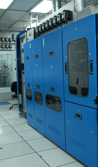
From prototyping to production to application engineering, we ensure excellence at every step of the GaN development process. Our state-of-the-art technology spans application-specific RF device and circuit designs, a differentiated set of GaN fabrication processes and MOCVD wafer production technology for end-to-end control over GaN device and circuits. Backed by 18+ years of R&D, we develop custom GaN wafers and devices that power use cases across the strategic and telecom sectors.
Vertically integrated excellence for best in class GaN solutions
Cutting-Edge GaN Technology
Developed through 18+ years of R&D at the Indian Institute of Science (IISc), Bangalore.
Cutting-Edge GaN Technology
Developed through 18+ years of R&D at the Indian Institute of Science (IISc), Bangalore.
Cutting-Edge GaN Technology
Developed through 18+ years of R&D at the Indian Institute of Science (IISc), Bangalore.
State-of-the-Art Manufacturing Technology
Differentiated manufacturing processes across the GaN wafer to circuits value-chain.
Stringent quality control measures to maintain reliability and consistency.
State-of-the-Art Manufacturing Technology
Differentiated manufacturing processes across the GaN wafer to circuits value-chain.
Stringent quality control measures to maintain reliability and consistency.
State-of-the-Art Manufacturing Technology
Differentiated manufacturing processes across the GaN wafer to circuits value-chain.
Stringent quality control measures to maintain reliability and consistency.
Innovation-Driven Approach
Backed by patent-protected technologies in GaN material design and device manufacturing.
Continuous advancements in GaN device technologies and application engineering for radio-frequency and microwave systems.
Innovation-Driven Approach
Backed by patent-protected technologies in GaN material design and device manufacturing.
Continuous advancements in GaN device technologies and application engineering for radio-frequency and microwave systems.
Innovation-Driven Approach
Backed by patent-protected technologies in GaN material design and device manufacturing.
Continuous advancements in GaN device technologies and application engineering for radio-frequency and microwave systems.
Trusted by Critical Industries
Delivering high-performance solutions for defense, aerospace, and telecommunications.
Designed to meet the demands of high-power, high-frequency, high-efficiency and compact GaN products for mission-critical applications.
Trusted by Critical Industries
Delivering high-performance solutions for defense, aerospace, and telecommunications.
Designed to meet the demands of high-power, high-frequency, high-efficiency and compact GaN products for mission-critical applications.
Trusted by Critical Industries
Delivering high-performance solutions for defense, aerospace, and telecommunications.
Designed to meet the demands of high-power, high-frequency, high-efficiency and compact GaN products for mission-critical applications.
Built for the Future
Enabling next-gen wireless transmit and energy-efficient power systems.
Committed to making GaN technology more accessible and scalable.
Built for the Future
Enabling next-gen wireless transmit and energy-efficient power systems.
Committed to making GaN technology more accessible and scalable.
Built for the Future
Enabling next-gen wireless transmit and energy-efficient power systems.
Committed to making GaN technology more accessible and scalable.
Precision. Performance. Perfection.
At AGNIT Semiconductors, we don’t just manufacture chips—we engineer reliability, performance, and innovation into every step. Our streamlined process, backed by cutting-edge technology and rigorous quality control, ensures that every semiconductor meets the highest industry standards.

01
Epitaxy
We grow a high-purity crystalline layer on a substrate, forming the foundation for semiconductor devices.

02
Device Processing
Using AGNIT’s advanced manufacturing processes, implemented with our foundry partners, we define device and circuit properties—from layout to electrical characteristics and everything in between.

03
Packaging
Semiconductor chips are enclosed in protective packaging to ensure durability, reliability, and optimal performance.

04
Reliability & Qualification
Our fully packaged RF HEMT devices undergo rigorous stress testing under real-world conditions to ensure exceptional stability, reliability, and long-term performance. This guarantees superior quality, durability, and customer satisfaction.
05
Evaluation Kits & Documentation
We provide evaluation kits and documentation for a complete demonstration of AGNIT packaged devices. Our experienced application team supports customers in the successful integration of AGNIT products into their systems.

06
Measurements
Precision instruments verify chip performance, efficiency, and compliance with quality standards.

07
Evaluation Kits & Documentation
We provide evaluation kits and documentation for a complete demonstration of AGNIT packaged devices. Our experienced application team supports customers in the successful integration of AGNIT products into their systems.
01
Epitaxy
We grow a high-purity crystalline layer on a substrate, forming the foundation for semiconductor devices.
02
Device Processing
Using AGNIT’s advanced manufacturing processes, implemented with our foundry partners, we define device and circuit properties—from layout to electrical characteristics and everything in between.
03
Packaging
Semiconductor chips are enclosed in protective packaging to ensure durability, reliability, and optimal performance.
04
Reliability & Qualification
Our fully packaged RF HEMT devices undergo rigorous stress testing under real-world conditions to ensure exceptional stability, reliability, and long-term performance. This guarantees superior quality, durability, and customer satisfaction.
05
Evaluation Kits & Documentation
We provide evaluation kits and documentation for a complete demonstration of AGNIT packaged devices. Our experienced application team supports customers in the successful integration of AGNIT products into their systems.
06
Measurements
Precision instruments verify chip performance, efficiency, and compliance with quality standards.
07
Evaluation Kits & Documentation
We provide evaluation kits and documentation for a complete demonstration of AGNIT packaged devices. Our experienced application team supports customers in the successful integration of AGNIT products into their systems.
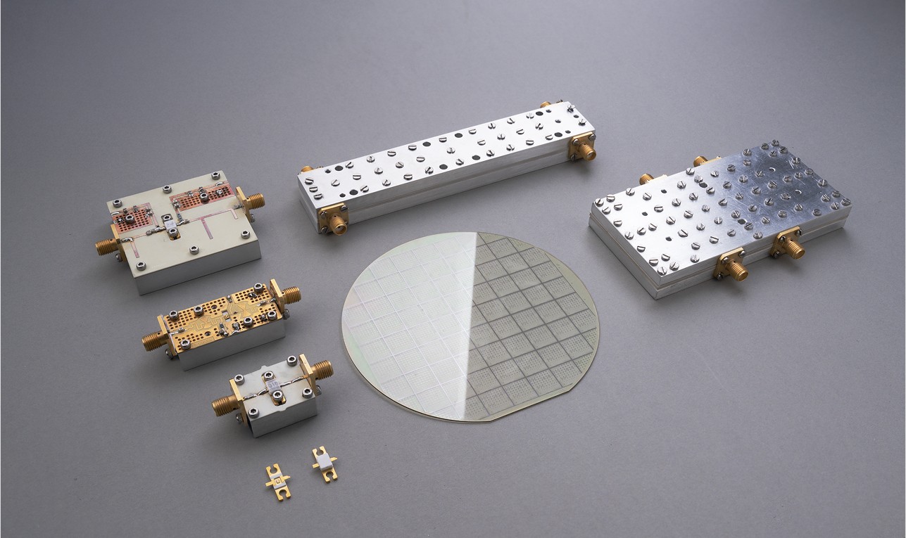
Gallium Nitride
Materials to Modules
Starting with wafers, AGNIT's technology and product portfolio includes devices, circuit design, and unique device processing.
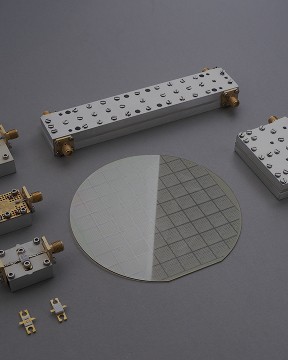
Gallium Nitride
Materials to Modules
Starting with wafers, AGNIT's technology and product portfolio includes devices, circuit design, and unique device processing.


Power up with GaN
Power up with GaN
2025 ©AGNIT Semiconductors Pvt. Ltd.
All rights reserved.
Power up with GaN
2025 ©AGNIT Semiconductors Pvt. Ltd.
All rights reserved.